Note: This board is no longer in production. It has been replaced with the new Version III ADC Board.
Notes:
- Other input impedance possible by changing one resistor pack
- User supplied short-wave receiver
- The current CPU firmware can be download from here
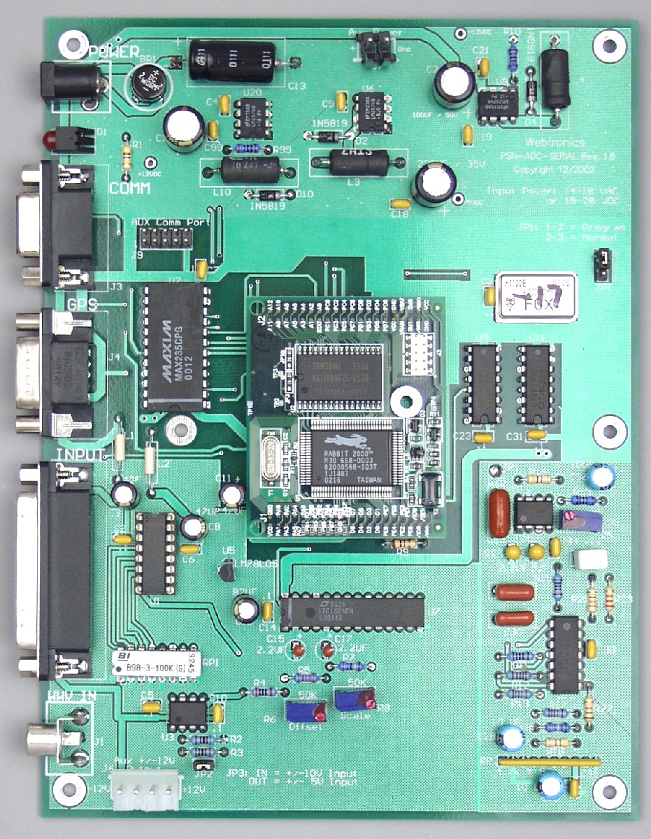
The PSN-ADC-SERIAL board comes with one DB-25 input connector and connector hood.
To order a board please contact me at the email address below.
WinSDR can be used to record data using the PSN-ADC-SERIAL board. This program is included with the purchase of the PSN-ADC-SERIAL board.
This Windows DLL Driver ( pdf version ) can be used by programmers who would like to write their own datalogger program or add the A/D board to an existing program. The driver zip file includes an example, written in VC++ 6.0, showing how to use the PSNADBoard.DLL file.
A device driver for the Windows version of Seislog is now available. Contact me for more information.
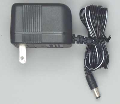
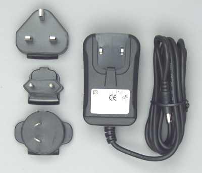
Power Supply Connector J5 and Power Requirements:
The power connector on the board is a standard 2.1mm X 5.5mm male jack. The board can be powered with either AC or DC voltages. The DC input range is 16 volts to 28 volts and the AC range is 11 to 18 VAC. At 16 VDC the board draws ~120 ma, at 25VDC ~95 ma and at 30VDC ~90 ma. If DC power is used, the center pin on the power connector can be connected to either the plus or minus voltage.
Note: If the user supplies their own power supply the voltage across the large capacitor C40 should be checked to verify there is enough voltage for proper operation. The voltage should be between 15 and 26 VDC, with ~18 VDC being optimum. If the voltage is too low, the DC regulators will not operate properly. If the voltage is too high, you will exceed the maximum voltage level of the parts on the A/D board.
Input Connector J2:
This connector is a 25 pin DB-25 female connector used for the 8 analog inputs and the 1 Pulse Per Second output signal used to verify the timing status. The connector has the following pinout:
- Pin 1 - Analog Input Channel 1
- Pin 2 - Analog Input Channel 2
- Pin 3 - Analog Input Channel 3
- Pin 4 - Analog Input Channel 4
- Pin 5 - Analog Input Channel 5
- Pin 6 - Analog Input Channel 6
- Pin 7 - Analog Input Channel 7
- Pin 8 - Analog Input Channel 8
- Pin 9 - Analog Ground
- Pins 10 and 11 - +12 VDC Output Power. 75 MA Max. - Note 1.
- Pin 12 - 1 Pulse Per Second TTL Output
- Pin 13 - Digital Ground
- Pins 14, 15, 16, 17, 18, 19, 20 and 21 Analog Grounds for Channels 1 to 8
- Pin 22 - Not Connected
- Pins 23 and 24 - -12 VDC Output Power. 75 MA Max. - Note 1.
- Pin 25 - Digital Ground
Note 1: PC board version 1.4 or higher. Not connected on earlier versions.
Comm Connector J4:
This connector is a 9 pin DB-9 female connector used to communicate to the PC running WinSDR. A straight through serial cable should be used between the A/D board and the your computer. The connector has the following pinout:
- Pin 1 - CD (Carrier Detect) Output - CPU P2-PC0 Line
- Pin 2 - Transmit Data Output
- Pin 3 - Receive Data Input
- Pin 4 - DTR (Data Terminal Ready) Input - CPU Reset Line
- Pin 5 - Ground
- Pin 6 - DSR (Data Set Ready) Output - CPU STAT Line
- Pin 7 - RTS (Request To Send), Connected to Pin 8
- Pin 8 - CTS (Clear To Send), Connected to Pin 7
- Pin 9 - Not Connected
GPS Comm Connector J3:
This connector is a 9 pin, DB-9 male connector used to communicate to a GPS receiver. A straight through serial cable should be used between the A/D board and the GPS's receiver interface board. See /gps/index.html for a GPS timing system compatible with the PSN-ADC-SERIAL board. The connector has the following pinout:
- Pin 1 - CD (Carrier Detect) Input, Used for the 1 PPS signal from the GPS receiver
- Pin 2 - Receiver Data Input from the GPS Receiver
- Pin 3 - Transmit Data Output to the GPS Receiver
- Pin 4 - +5 VDC for Garmin GPS 16 Power - Note 1
- Pin 5 - Ground
- Pin 7 - Ground for Garmin GPS 16 - Note 1
- Pins 6, 8 and 9 - Not Connected
Note 1: PC board version 1.5 or higher. Not connected on earlier versions.
WWV In Connector J1:
This connector is a RCA Jack used for the WWV audio input from the short-wave receiver tuned to one of the WWV stations. For more information on using the WWV option please see the SDR documentation here /sdrdocs/wwvcorr.htm.
The board has three jumpers. They are:
JP1:
Used to enable programming of the flash memory on the microprocessor board. The jumper on JP1 should only be places between pins 1 and 2 when upgrading to new firmware on the CPU board. This jumper must be placed between pins 3 and 4 for normal operation of the A/D board.
JP2:
This connector is used a third comm port. Currently the firmware on the A/D board uses this comm port as a time server. See this SDR Documentation page for more information.
Pinout:
- Pin 3 - Transmit Data Output
- Pin 5 - Receive Data Input
- Pin 9 - Ground
- Pins 1, 2, 4, 6, 7, 8 and 10 - Not connected
JP3:
This jumper controls the input voltage range of the A/D converter. When the jumper is in, the input voltage range is +- 10 volts. With the jumper removed, the input range is +- 5 volts. The jumper controls all 8 analog input channels.
CPU firmware versions 2.4 and above support a special mode that allows GPS mapping programs like WinPlotGPS to communicate directly with the GPS receiver attached to the A/D board. When the A/D board is placed in the pass-through mode, all serial data (the 1PPS signal is not passed through) from the GPS receiver is sent out the Comm Port and all data sent to the Comm Port will go to the GPS receiver. Note, in this mode the board will not record or send out A/D data.
This 32-Bit Command Line (Windows DOS Box) program passthru.exe is currently the only one way to force the A/D board into the Pass-Through mode. See the readme file contained in the zip file for more information.
When the A/D board receives the Pass-Through mode command, the baud rate of the Comm Port on the A/D board will be changed to 4800 or 9600. The baud rate will be set to 4800 if the GPS receiver outputs NMEA text messages or 9600 if the receiver outputs the Motorola binary format.
This page viewed times since November 29, 2001